Senajith “Seno” Rekawa grew up in Sri Lanka and moved to the United States in 1989, where he attended Diablo Valley College and then the University of Wisconsin–Madison. He first came to Berkeley Lab in 1991 as a summer intern, where he helped build the storage ring at the Advanced Light Source (ALS).
Rekawa is now Chief Engineer and Deputy Director at the Center for X-Ray Optics (CXRO), a state-of-the-art testbed developing extreme ultraviolet lithography systems to address national needs. His honors include a Director’s Award in 2021, an ALS Division Instrumentation (Halbach) award, and the American Society of Precision Engineering’s 2025 Distinguished Service Award in 2025. He also held several leadership positions, including President (2022) of the ASPE.
Outside the Lab, Rekawa serves on the advisory committee of the engineering department at San Jose State University, advises companies engaged in extreme ultraviolet (EUV) instrumentation development, and provides engineering support to NIST and other U.S. national laboratories. He has also coached soccer and rugby for his son’s teams, and supports Sri Lanka whenever possible, contributing to hospitals, assisting students and schools, and helping underserved and less fortunate communities.
When did you first become interested in engineering?
As a child, I was always a mechanical person. My family is all lawyers and judges. That may have even pushed me toward engineering because I was always listening to this boring lawyer talk at the dinner table. I’m the only person in my family who is interested in the technical stuff. When I was 11 or 12, I had a Mini Moke that I used to take apart and modify. If anything broke around the house — oven, microwave, washing machines — I was the one to fix it. From 1987 to 1990, there was a civil war in Sri Lanka. I decided to move to the United States right after high school.
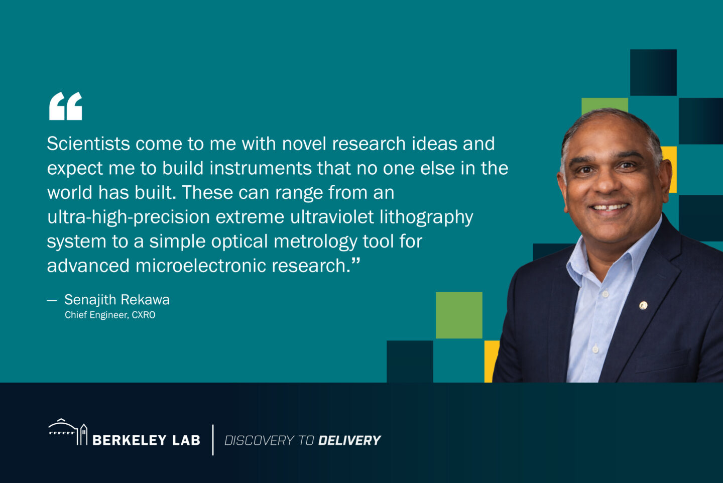
What do you do at the Lab?
Scientists come to me with novel research ideas and expect me to build instruments that no one else in the world has built. These can range from an ultra-high-precision extreme ultraviolet lithography system to a simple optical metrology tool for advanced microelectronic research. I would then look at what it is they want and what they need, and come up with a project plan, assemble a team of experts, and start designing and building. We really need to understand the specifications and take a step back and say, how do we get there? Most of the tools are designed to print or image features close to 8 nanometers – 100,000th of a hair – vibration and temperature stabilities are critical in designing high-precision motion systems. For example, we recently developed the world’s highest resolution projection lithography tool (MET5) for semiconductor research.
How has the Lab changed since you started as a full-time employee in 1995?
It’s changed quite a bit but many things have stayed the same. We are building a really good safety culture. There is now more planning for projects since we need to include asking if the infrastructure can support the project and what is the best timing for the project.
Discovery to Delivery is a Berkeley Lab communications campaign showcasing how we are turning decades of fundamental discoveries into real-world impact with benefits to Americans in their everyday lives. From accelerating advancements in microelectronics and quantum to artificial intelligence, and more, explore how teams across the Lab are powering the breakthroughs of tomorrow on the Discovery to Delivery website.
